| SSD Technology |
|
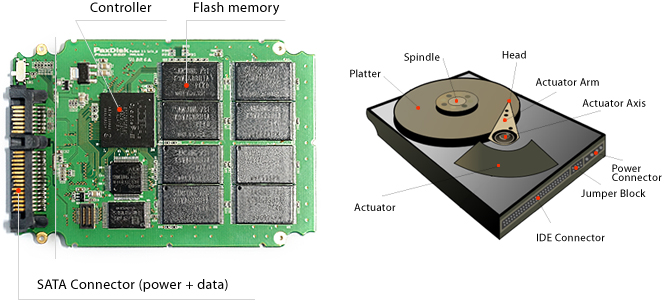
| ㆍ Solid-State Drive (SSD) is a non-mechanic semiconductor storage compatible with HDD. |
| ㆍ NAND Flash SSD has a controller emulating HDD, through flash memory array. |
|
|
|
|
|
| ■ Physical feature of Flash Memory |
|
| ㆍ Just like ROM(read only memory), when power off, the DATA of memory is not erased. |
| ㆍ Just like DRAM/SRAM, read/write is faster than HDD. |
| ㆍ It is rugged, shock-resistent and operating temerature scope is more wide than HDD |
|
|
|
| ■ Technical feature of Flash Memory |
|
| ㆍ Must erase before write. |
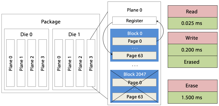
| ㆍ The unit of read/write and erase is different each other- Read/Write per page (2 to 8KB), Erase per block (128 pages) |
| ㆍ Time to read, write, erase is also different.- Read (0.025ms) < write (0.2ms) < erase (1.5ms) |
| ㆍ To erase is executed separately by internal request |
| ㆍ The flash memory life cycle is limited because erasing wears out the memory. |
|
|
|
| * NOR Flash |
|
| ㆍ Random, direct access |
| ㆍ Random reading speed is fast |
| ㆍ Write and erase is slow |
| ㆍ Perfect for storing program code |
|
| * NAND Flash |
|
| ㆍ I/O Access by Page unit |
| ㆍ Low price, High Density |
| ㆍ Erase and write is better than NOR |
| ㆍ Perfect for storing sequential data |
|
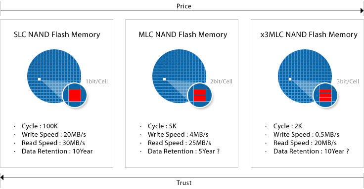
| ■ SLC vs. MLC |
|
| ㆍ SLC has 1 bit per memory cell, MLC NAND Flash chip has 2 bit per memory cell. |
|
|
|
| ㆍ SLC has more reliability than MLC, so it is possible to read/write 100k times, but expensive. |
| ㆍ MLC can read/write only several thousand times, But it is good for mass product due to its low price. |
| ㆍ SLC is usually used by industrial and defense application. |
|
|
|
| ■ The Physical Structure of NAND Flash |
|
| ㆍ Reading is very fast but writing is slow, so buffer utilization is used by SSD controller for efficiency |
| ㆍ It takes a long time to erase, the controller does the background erase at once in order not to affect the overall performance. |
|
|
|
|
|
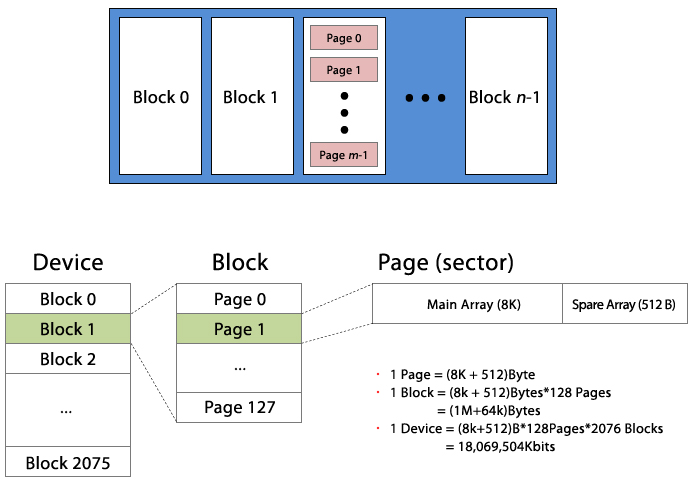
| ■ The Logical Structure of NAND Flash Memory |
|
| ㆍ NAND Flash can be accessed only by the Block unit and its sub-structure Page unit, if you use only one byte, you have to use entire page |
|
|
|
|
|
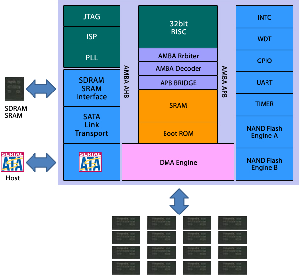
| ■ SSD Architecture |
|
SSD Controller is a kind of SoC (system on chip) to Host (computer),
So can control the flash memory independently to provide a stable storage performance. |
|
|
|
|
|
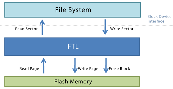
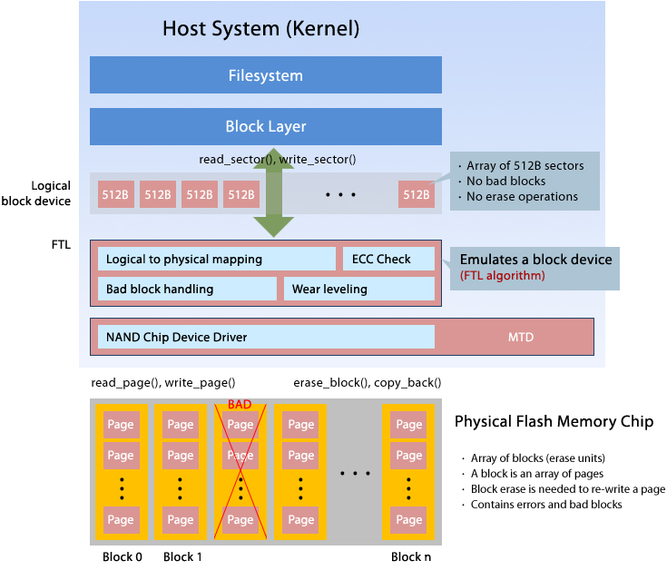
| ■ FTL(Flash Translation Layer) |
|
| ㆍ Hide operating charateristics |
| ㆍ Provide general file system interface |
| ㆍ Embedded SW to emulate flash memory to HDD |
|
|
|
FTL converts the logical address to the actual physical address of Flash memory, as well as convert the reverse,
to hide its charateristics is a key role because flash memory writing operation is to be delayed. |
|
|
|
| ■ NAND Flash SSD Architecture |
|
The various technical elements of SSD are required to extend the life span of the Flash memory. |
|
| ㆍ Garbage Collection has similar function just like Windows disk defragmentation on a PC. |
| ㆍ ECC is stored to a separate area, when error occured, it can do automatic recovery to take advantage of the stored code. |
| ㆍ Bad block management performs a similar role in the background, just as a HDD low level format confirms available storage area |
| ㆍ When you continue to write in a certain area of Flash memory by repeating it, |
| ㆍ the specific area of the momory cell is damaged, |
| ㆍ so Wear leveling helps to write evenly the entire flash memory cell automatically. |
|
|
|


